1.Understanding PCB Boards: The Backbone of Electronic Devices
Printed Circuit Boards (PCBs) stand as the unsung heroes of the electronic realm, providing an essential infrastructure for the functionality of a myriad of devices encountered in our daily lives. This section delves into the intricate details of PCB boards, illuminating their construction, design principles, and the pivotal role they play in modern electronics.
Anatomy of a PCB Board
At the core of every electronic device lies a meticulously crafted PCB board, akin to the central nervous system of the device. These boards typically consist of multiple layers of non-conductive substrate material, commonly fiberglass, laminated together with thin layers of copper foil. The copper traces form an elaborate network, serving as the pathways for electric currents that bring devices to life. A protective layer called solder mask shields the board from environmental factors, ensuring the integrity of the circuitry.
To illustrate, consider the motherboard of a computer. It encapsulates a complex PCB that integrates various components, such as the central processing unit (CPU), memory modules, and peripheral connectors. The meticulous arrangement of traces and components is designed to facilitate efficient communication between these elements, creating a cohesive and functional unit.
Design Principles: A Balancing Act
Creating a PCB board is a delicate dance between functionality, efficiency, and spatial constraints. Engineers must intricately design the layout of components, taking into account factors such as signal integrity, power distribution, and thermal management. Advanced design software, such as Altium Designer or Eagle, is instrumental in optimizing these aspects.
Imagine designing a PCB for a medical device that requires high precision and reliability. The layout must be carefully orchestrated to ensure that signals between sensors and processing units are not compromised. Additionally, the design must consider the spatial constraints of the device, emphasizing the importance of a meticulous balance between form and function.
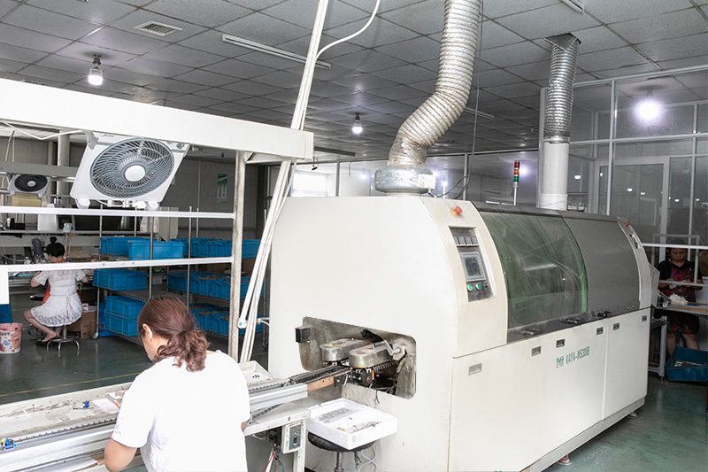
PCB Manufacturing: Precision at Scale
Once the design is finalized, the manufacturing process commences. This involves etching the copper layers according to the design specifications, drilling holes for component placement, and applying various finishes to enhance durability and conductivity. Modern manufacturing techniques, such as surface mount technology (SMT) and through-hole technology (THT), enable the production of PCBs with unprecedented precision.
Consider the mass production of smartphones. The intricate PCBs within these devices undergo a high-volume manufacturing process that demands precision and reliability. Automated assembly lines handle the intricate soldering of tiny components, ensuring consistency and efficiency in the production of millions of devices.
2.Evolving Trends in PCB Technology: From Miniaturization to Flexibility
As technology advances, so does the evolution of PCB boards. This section explores the latest trends shaping the world of PCB technology, from miniaturization to the rise of flexible PCBs, showcasing how these innovations are redefining the landscape of electronic design.
Miniaturization: The Quest for Compactness
The demand for smaller and lighter electronic devices has propelled the trend of miniaturization in PCB design. Engineers are challenged to pack more functionality into increasingly compact spaces. Microvias, tiny openings in the PCB that allow for more precise routing, and advanced routing techniques allow for higher component density.
Consider the evolution of laptops. Over the years, there has been a remarkable reduction in size and weight, driven by advancements in miniaturization of PCBs. Compact PCBs house powerful processors, memory modules, and other components, contributing to the sleek and portable design of modern laptops.
Flex PCBs: Bending the Rules
Flexible PCBs represent a paradigm shift in electronic design. Unlike traditional rigid boards, flex PCBs are made from flexible materials, enabling them to bend and conform to irregular shapes. This flexibility opens up new possibilities in product design, especially in industries such as wearables, automotive, and medical devices.
Take, for example, a wearable fitness tracker. The flexible PCB within the device allows it to wrap around the user's wrist comfortably. This form of PCB enables the creation of wearable technology that seamlessly integrates with the contours of the human body, demonstrating the versatility and innovation made possible by flexible PCBs.
Integration of IoT and Smart PCBs
The Internet of Things (IoT) has ushered in an era where devices are interconnected and communicate seamlessly. Smart PCBs, equipped with embedded sensors and communication modules, play a pivotal role in enabling this connectivity. From smart home devices to industrial automation, the integration of IoT into PCB design enhances functionality and opens up new avenues for innovation.
Consider a smart home system where various devices, such as thermostats, lights, and security cameras, are interconnected. Smart PCBs within these devices enable communication and coordination, allowing for a synchronized and intelligent home automation system. This integration not only enhances convenience but also showcases the interconnected nature of modern electronic devices.
3.Ensuring Reliability: PCB Testing and Quality Assurance
The final frontier in the journey of a
PCB board is ensuring its reliability and functionality. This section explores the critical aspects of PCB testing and quality assurance, emphasizing the importance of these processes in guaranteeing the longevity and performance of electronic devices.
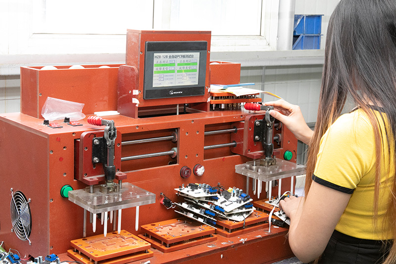
Testing Protocols: From Prototype to Production
Comprehensive testing protocols are implemented at various stages of PCB development, from the prototyping phase to mass production. Functional testing, which involves verifying that the PCB performs its intended functions, is a critical step. Boundary scan testing and in-circuit testing are methods employed to identify defects and ensure that the board meets the specified performance criteria.
Consider the testing of a PCB for a high-reliability aerospace application. Rigorous testing ensures that the PCB can withstand the harsh conditions of space, including temperature extremes and radiation. The testing process is not only about identifying defects but also about validating the performance of the PCB under real-world conditions.
Quality Assurance: Meeting Industry Standards
Adherence to industry standards is paramount in ensuring the quality and reliability of PCBs. Certifications such as IPC-A-600 for bare boards and IPC-A-610 for assembled boards set the benchmark for quality assurance. Manufacturers invest in quality control measures, including automated optical inspection (AOI) and X-ray inspection, to detect defects that may compromise the functionality and longevity of the PCB.
Consider a medical device that must meet stringent quality standards to ensure the safety of patients. The PCB within such a device undergoes rigorous quality assurance processes to comply with regulatory requirements and industry standards. This commitment to quality assurance is not just a box to check; it is a fundamental aspect of ensuring the reliability and safety of electronic devices.
Environmental Considerations: Sustainable PCB Design
In an era of increasing environmental awareness, sustainable and eco-friendly practices are becoming integral to PCB design and manufacturing. RoHS (Restriction of Hazardous Substances) compliance and the adoption of lead-free solder are examples of industry initiatives aimed at reducing the environmental impact of electronic devices. Sustainable practices not only align with regulatory requirements but also contribute to the broader goal of creating a more environmentally conscious electronics industry.


